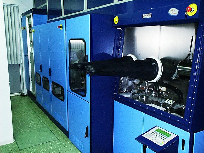
Multi-Layer 3-5 Material EPI by MOCVD
The Institute for Electronic Materials Technology (ITME) in Warsaw, Poland is able to undertake the preparation of custom EPI layers (one or multi-layer structures) on any 3-5 materials and they actively seek such work. Please contact us for a quotation for a specific structure.
As an example of a routinely produced EPI wafer we quote:
- Wafer: 2"Ř with InGaAs EPI on SI InP <100>, by MOCVD deposition
- Substrate: Semi-Insulating InP (eg. InP:Fe),
- Resistivity: > 1 × 10E7 Ohm cm, EDP < 1 × 10E4/cm2
- EPI: Lattice matched In/Ga alloy layer of
n-type InGaAs
- Nc > 2 × 10E18/cc (using Si as dopant)
- Thickness: 0.5 µm (+20%)
- Price: $1,200.00 each (for 1 to 10 wafers),
- Delivery: 5 weeks ARO
For more information contact EL-CAT Inc. at el-cat@el-cat.com.
Multi-Layer 3-5 Material EPI by MOCVD
The Institute for Electronic Materials Technology (ITME) in Warsaw, Poland is able to undertake the preparation of custom EPI layers (one or multi-layer structures) on any 3-5 materials and they actively seek such work. Please contact us for a quotation for a specific structure.
As an example of a routinely produced EPI wafer we quote:
- Wafer: 2"Ř with InGaAs EPI on SI InP <100>, by MOCVD deposition
- Substrate: Semi-Insulating InP (eg. InP:Fe),
- Resistivity: > 1 × 10E7 Ohm cm, EDP < 1 × 10E4/cm2
- EPI: Lattice matched In/Ga alloy layer of n-type
InGaAs
- Nc > 2 × 10E18/cc (using Si as dopant)
- Thickness: 0.5 µm (+20%)
- Price: $1,200.00 each (for 1 to 10 wafers),
- Delivery: 5 weeks ARO
For more information contact EL-CAT Inc. at el-cat@el-cat.com.