Frequently Asked Questions
Find answer to your question about semiconductor materials.
There are 4 main dopants B, P, Sb and As for CZ Si. Common resistivity ranges are:
| Dopant: | Resistivity: | Chart: |
|---|---|---|
| Boron: | 0.001-140 Ώ cm |  |
| Phosphorus: | 0.03-140 Ώ | |
| Antimony: | 0.008-0.600 Ώ cm | |
| Arsenic: | 0.001-0.005 Ώ cm | |
| 0.001-0.004 Ώ cm | ||
| 0.002-0.003 Ώ cm |
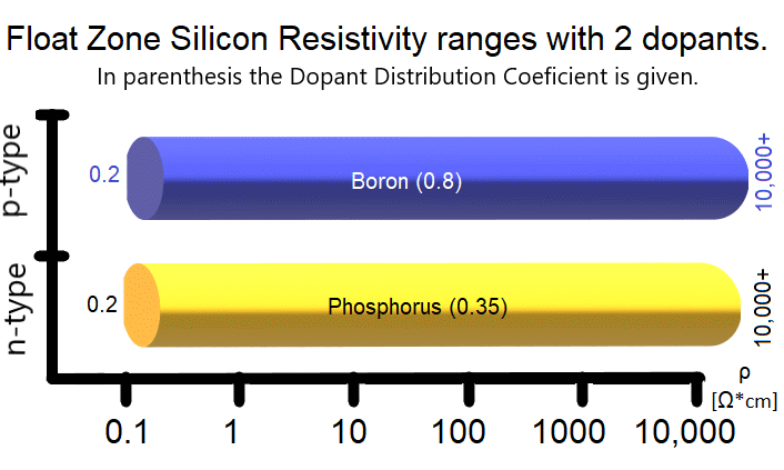
There are 2 main dopants B, P for FZ Si. Common resistivity ranges are:
| Dopant: | Resistivity: | Chart: |
|---|---|---|
| Boron: | 0.2-10000+ Ώ cm |
|
| Phosphorus: | 0.01-10000+ Ώ cm |
The Si wafer surface roughness is guaranteed by repetition of the
chemical-mechanical-planarization (CMP) polishing process, not by any measurement, which
would be destructive. For the polished side of the wafers the normal roughness value is
<0.5nm (<5Å). Any standard Quality Certificate doesn't mention any surface roughness
measurements data as the roughness is guaranteed by repetition of the
chemical-mechanical-planarization (CMP) polishing process.
Common way to measure roughness is with use of Atomic Force Microscope (AFM).
We offer AFM measurements as the service.
NTD FZ stands for Neutron Transmutation Doped Float Zone silicon. NTD is
the silicon doping technique. The NTD process takes place when undoped (high purity)
mono-silicon rods are irradiated in a thermal neutron flux inside nuclear reactor. The
thermal neutron is captured by the 30Si atom, which has a 3% abundance in pure Si. Due
to the high neutron/proton ratio of 31Si, it will release a beta and, by converting a
neutron to a proton, the Si-31 atom transmutes to a P-31 atom according to this
reaction:
30Si + n → 31Si → (β-) 31P.
In the result Phosphorus (n-type) doped silicon, with the lowest resistivity variation of any crystalline silicon product on the market is created.
- Thermal Silicon Oxide is SiO2 grown by oxidizing the silicon of the wafer itself. This form a hard and dense SiO2 that is essentially monocrystalline. Thickness range is wide: from 100Å to 50000Å
- Low Temperature Oxide (LTO) or Chemical Vapor Deposition (CVD) deposited SiO2 is a soft porous SiO2, used on silicon wafer back-side to absorb impurities during Epi growth.
- Sputtered SiO2 form a polycrystalline deposited layer that can be grown as thick as 5 or 10µm.
- Electron Beam Evaporated SiO2 is glass-like but is limited to about 2µm of thickness.
Each of these SiO2 layers, although chemically the same, actually have significantly different physical properties. It is the customer who decides what oxide is needed
Oxygen dissolved in Silicon is measured according to ASTM F-1188 by IR absorption using
FTIR.
However this measurement only works for Silicon with resistivity > 0.1 Ohmcm. At lower
resistivities
IR absorption is too high to get a meaningful measurement. For low resistivity wafers,
oxygen content
is reported as measured on higher resistivity Silicon made under the same conditions.
For critical applications
SIMS measurement method is required to mesure bulk oxygen content. However, we can say
that for typical Czochralski
process expected oxygen content is within 24-38 ppma (ASTM F121-76) limits.
Examples of controlled Oxygen groups:
- O2 from 31.0 to 36.8 ppma (<111> orientation)
- O2 from 28.0 to 32.0 ppma (<100> orientation)
- O2 from 29.0 to 35.0 ppma (<100> orientation)
If Low Oxygen content is critical for your application then we recommend using FZ crystallized Silicon. Then FZ silicon Oxygen content is < 1ppma.
Undoped GaP conductivity type is 'n', which is different to silicon. Intrinsic Si type remain unknown for undoped (can be 'p', can be 'n').
Resistivity, Charge Carrier Concentration and Mobility are related, as follows:
Ro=1/(k × Nc × u)
where Ro is resistivity in Ohm cm
k is charge of a Charge Carrier in Coulombs per Charge Carrier {Charge of an
electron}
Nc is Number of Charge Carriers per cm³
u is Charge Carrier Mobility in cm² per Volt Sec
You can check the units
Ro = [Ohm×cm] = [Volt/(Ampere×cm)] = [Volt/(Coulombs/Sec)×cm] =
[(Volt×Sec×cm)/Coulomb]
k = [Coulomb/Atom] {One Dopant atom contributes one electron or hole charge
carrier}
Nc = [Dopant Atoms/cm³]
u = [cm²/(Volt×Sec)]
k = 1.602E-19 Coulombs (Charge of an electron - a constant of nature)
The table below gives dependance between concentration and mobility for III-V
Compound Semiconductors:
| Doping of III-V Compound Semiconductors | |||||||||||||
|---|---|---|---|---|---|---|---|---|---|---|---|---|---|
| Undoped | Doped n-type | Doped p-type | Semi-Insulating | ||||||||||
| type | Nc [a/cm3] |
Mobility [cm2/Vs] |
Nc [a/cm3] |
Mobility [cm2/Vs] |
Nc [a/cm3] |
Mobility [cm2/Vs] |
Ro [Ohm-cm] |
Mobility [cm2/Vs] |
|||||
| GaAs | GaAs:- | n | 1E7-3E8 | 6,000 - 3,000 | GaAs:Si | 1E16-4E18 | 3,000-1,000 | GaAs:Zn | 1E16-4E19 | 210-50 | GaAs:Cr | 1E7-1E9 | 2,000-4,500 |
| GaP | GaP:- | n | 1E12-3E16 | 170 - 140 | GaP:S | 3E17-8E18 | 140-100 | GaP:Zn | 6E17-6E18 | 66-56 | GaP:- | 1E7-1E12 | 140-160 |
| GaSb | GaSb:- | p | 1E16-2E17 | 3,000 - 600 | GaSb:Te | 5E16-5E18 | 3,500-2,000 | GaSb:Zn | 1E18-7E18 | 500-275 | |||
| InAs | InAs:- | n | 2E16-6E16 | 25,000-21,000 | InAs:S | 5E17-2E19 | 14,800-6,000 | InAs:Zn | 1E18-4E19 | 155-96 | |||
| InP | InP:- | n | 5E14-3E16 | 4,500-1,700 | InP:S | 3E18-9E18 | 1,600-1,000 | InP:Zn | 4E18-6E18 | 60-50 | InP:Fe | 1E7-9E7 | 1,700-3,200 |
| InSb | InSb:- | n | 1E14-5E14 | 500,000-350,000 | InSb:Te | 1E15-2E18 | 200,000-24,000 | InSb:Ge | 1E15-5E17 | 70,000-4,000 | |||
Notes:
- InSb parameters measured at 77K, all others at 300K
- Undoped GaAs:- is normally Semi-Insulating, ultra-pure GaP is Semi-Insulating, none of the others are
- Mobility is that of Majority Charge Carriers; p-type Mobility is Hole Mobility, all others are Electron Mobility
To recalculate from Sheet Resistance in [Ohms/square]
to Resistivity [Ohm-cm] the Rs=Ro/t
formula is used
where:
t is wafer thickness,
Rs is sheet resistance Ohms/square,
Ro is resistivity in Ohm-cm.
An "Epi-ready" surface is one that was polished and cleaned to be free of microscopic particles, such that an Epi layer can be grown on the surface. Even if the wafers deliveried are certified to be 'epi-ready' it is good industry practise to clean the wafers just before processing.
SEMI refers to the SEMI Organization (https://www.semi.org/) which specifies the standards for silicon wafers and other semiconductor materials. "Prime" and "Semi Prime" wafers are equivalent and the highest grade of a silicon wafer. SEMI organization indicates the bulk, surface and physical properties required to label silicon wafers as "Prime Wafers". "Test" or "Semi Test" wafers are virgin silicon wafers of lower quality than Prime and used primarily for testing processes. SEMI organization indicates the bulk, surface, and physical properties required to label silicon wafers as "Test Wafers". Unlike "Primes" the "Test" wafers may show some surface defects (like scratches, LPDs or particles) or bulk defects (like excessive EPD or impurities).
- All prices are in US Dollars.
- All prices are rounded to the tenths of Dollar.
- Shipping costs and customs fees are not included into material prices.
- Selling full boxes of wafers is preferred. If smaller quantity (below full box) is needed the clean room repacking fee is applied and included into the wafers price. The price is recalculated accordingly.
- The repacking fee for silicon wafers with 8" diameter is higher than regular repacking fee.
In stock Si wafers have no minimum order quantity (no MOQ) and we are happy to
deliver just one wafer. However, we apply a clean room repacking fee for each box we
have to repack. The split cassette fee is $150/box for all diameters below
Ø8" (<200mm) and $250/box for Ø8" (=200mm).
We do not repack Ø12" (=300mm) and any larger diameter wafers.
We also offer made-to-order Si wafers and specialize in small quantities.
The MOQ for made-to-order depends on the
specifications (please click)
that we shall agree before offering.
To correctly display downloaded file:
- Open MS Excel.
- Open new empty sheet (data workbook).
- Open the "Data" tab.
- Import data from the text file downloaded.
- Select UTF-8 encoding.
- Set all column types to text.
- Enjoy.
Notes:
- Our CSV files use semicolons ";" as delimiters (column separators).
- All files use UTF-8 encoding.