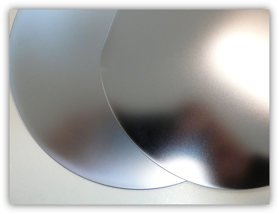
Silicon wafers are the basic raw material from which transistors, integrated circuits, memory chips, microprocessors and various other semiconductor devices are made, for use in electronics, familiar to us in everyday use. Wafers are made from ultra pure silicon, crystallized by the Czochralski or Float Zone methods, into single crystal ingots. These ingots are sliced into thin wafers, then lapped, etched, polished and cleaned, to become the purest, flattest, smoothest and cleanest objects possible. Only such perfections can yields the billions of submicroscopic transistors that make up modern semiconductor devices.
How are silicon wafers made?
Introduction
From sand to ingot
Silicon (at 27%) is the second most abundant element in earth's crust (after oxygen). It is never found as the elemental silicon, but as the compound SiO2. It is the main constituent of sand and many rocks.
Semiconductor applications of silicon require extraction and
purification of this element to level of ~99.9999999% (9N).
It takes the following three energy-consuming steps:
| Sand to Metallurgical grade Silicon | Metalurgical to Semiconductor grade Silicon (Siemens process) | Monocrystalline Silicon ingots |
|---|---|---|
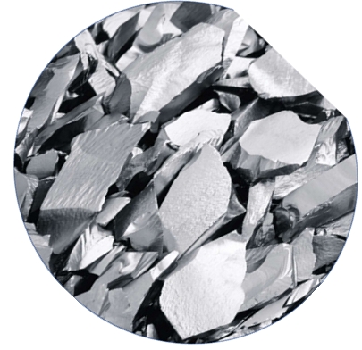
| Naturally occurring silica sand (at least 98% SiO2) is mined where convenient for transport by ships (eg. Mexico), and carried to where hydroelectric power is plentiful and cheap (eg. west coast of Norway). There it is charged into electric arc furnaces with massive carbon electrodes where at a high temperature Silicon is produced according to SiO2+2C→Si+2CO This is metallurgical grade Silicon (99% pure) for use in hardening of Aluminium and Steel. | Metallurgical grade Silicon is reacted with hydrogen chloride to produce compounds of Silicon, Chlorine and Hydrogen typically: Si+3HCl→SiHCL3+H2 (called Trichlorosilane or TCS), which is a liquid, is then distilled through many stages from initial 2N to the amazing 9N purity. Ultra-pure TCS vapour is pumped over Silicon rods heated to 1,150ºC where it dissociates and Silicon deposits on the rods as tiny crystals. Remaining volatile compounds are redistilled and recycled. The silicon rods, when grown to 100mmØ or 200mmØ, are removed and used for FZ crystallization or crushed into smaller chunks for use in the CZ crystallization process. This is the Siemens process, which is most widely used to make semiconductor grade Silicon. | The polycrystalline silicon is recrystallized into monocrystalline ingots. The most commonly used is the Czochralski (CZ) process. In it the polysilicon chunks and an appropriate dopant are charged into a quartz crucible and melted under Argon in an electric furnace. A seed crystal is inserted then slowly rotated and withdrawn while the Silicon crystallizes about it, forming a cylindrical monocrystalline ingot of desired diameter of up to Ø300mm or even Ø450mm. Crystallographic orientation of the ingot is that of the seed crystal {(100), (111), (110) or (211)}. The dopant added in a small but precise amount of Boron or Phosphorus or Antimony or Arsenic which gives the material specific type and degree of electrical conductivity. The floating zone (FZ) technique is a crucible-free crystal growth method. In FZ growth, the molten zone is kept between two vertical solid rods by its own surface tension. Dopant is introduced by blowing a gas containing the dopant element into the melt zone. FZ is used only for very high resistivity ingots or to avoid the trace amounts of Oxygen that dissolve into Silicon from the quartz crucible in CZ method. |
From ingot to wafer
Silicon ingots are made in various sizes (commonly in nominal diameters of 1", 2", 3", 100mm, 125mm, 150mm, 200mm, 300mm and 450mm). They are either CZ or FZ crystallized. Ingot crystallographic orientations are usually (100) or (111) and sometimes (110) or (211). Silicon ingots are doped with Boron (B) to have p-type resistivity of anywhere from 0.001 to 10,000 Ohmcm {most commonly (1-10)}. To have n-type resistivity Silicon is doped with Phosphorus. Resistivities from 0.001 to 10,000 Ohmcm are possible, but resistivities below 0.1 Ohmcm require certain safety precautions in manufacture. Antimony (Sb) is used to dope Silicon to n-type (0.008-0.020)Ohmcm and Arsenic (As) to dope Silicon to n-type (0.001-0.005)Ohmcm. Undoped (intrinsic) Silicon ingots can have resistivity > 20,000 Ohmcm and then type is indeterminate. CZ crystallized Silicon ingots Boron doped to (0.1-100)Ohmcm range, have to be heat treated (quenched) after crystallization to eliminate Boron-Oxygen complexes that grow during slow cooling. This is done routinely for ingots not more than 4"Ø. Such material more than 4"Ø, has to be heat treated as wafers after slicing, since large ingots cannot be cooled fast enough. All electronic properties of Silicon wafers are determined in the manufacture of ingots. Wafer manufacture affects only the geometric properties and crystallographic parameters of wafers. Silicon ingots are made into Silicon wafers in the following precision major manufacturing steps:
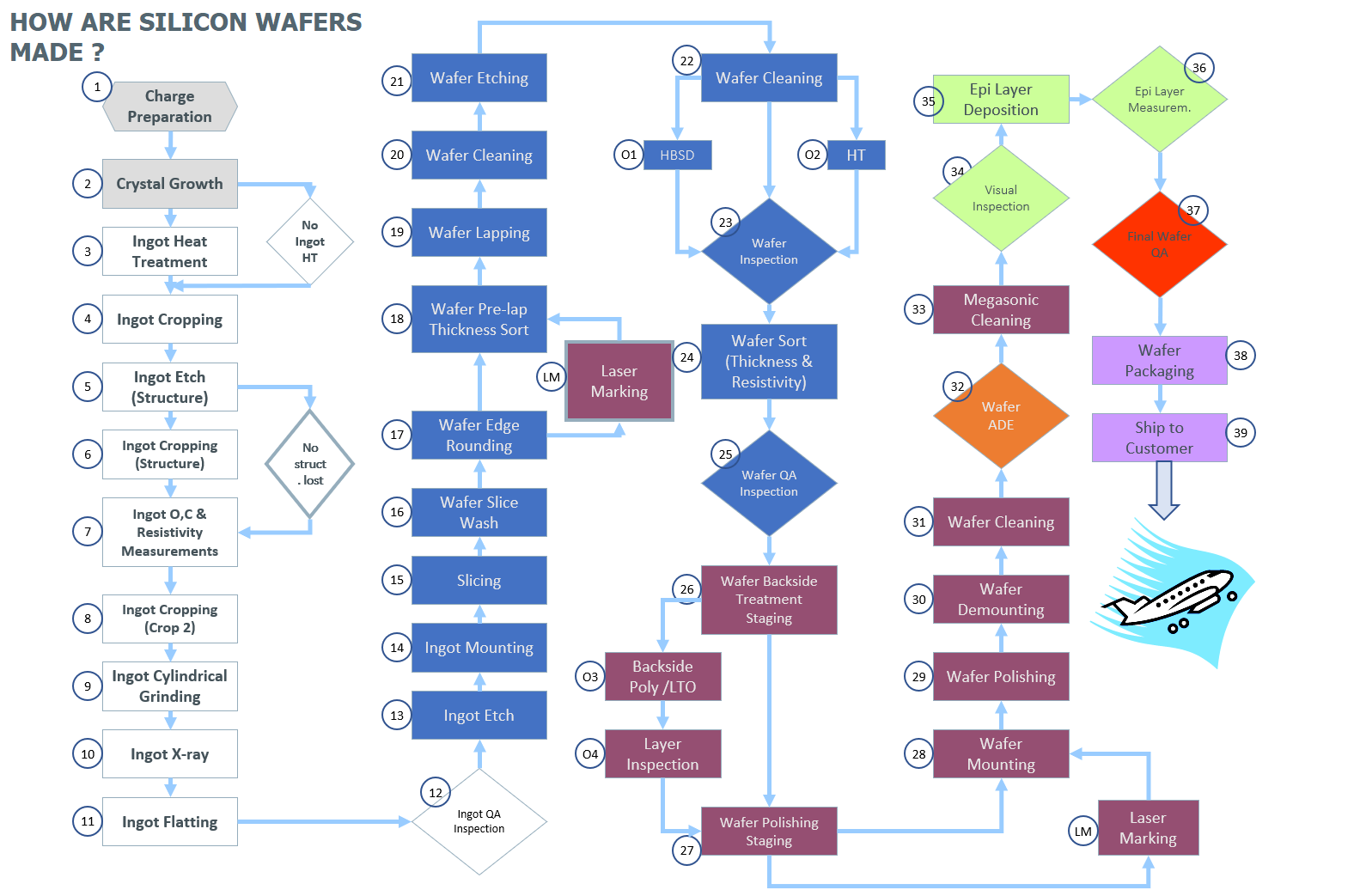
| Ingot slicing | Wafer edge rounding | Wafers lapping & etching | Wafers polishing |
|---|---|---|---|
| Ingots, after the growth, are top and tail cropped, grounded to the diameter and sliced into wafers. There are two slicing methods in use, wire slicing, commonly used in a mass production and ID slicing, apllied for short series. During slicing the ingots are often tilted from their axis to create off-oriented wafers. Off orientation is crucial for some applications (e.g. to zero diffraction plates for X-ray), also improves smooth epitaxial growth of silicon on silicon layers. | To prevent chipping, the sharp edge of the wafer is grinded to the round shape. There are many edge shapes are possible and applied for different applications. Long, sharp edges improves smooth epitaxial silicon growth, and are often apllied for substrates used for thick epi layer (>20µm). Trapesoidal edge shape is used for very thick wafers (>3000µm). Such wafers 'sliced and edge-rounded wafers' are called 'as-cut' wafer. | The wafers are sorted into thickness groups, loaded into batch lapping machines and lapped. Quartz based and fine lapping powders are used. After the process the wafer are uniform in thickness, surface appereance and shape but require etching to remove all subsurface mechanical damages. Two types of etching are in common use: alkalline (with KOH solution use) and acid (with HNO3, CH3COOH and HF mixture). Wafers after these processes are called "as-etched". "As-etched" wafers are good enough to be used as the start wafers to produce devices (e.g. thyristors). | But majority of the aplications require smoother, mirror-like polished surface, with Ra less than 5 Angstroms. To achieve such surface, Si wafers are chemical-mechanical-polished. In a standard process, Si wafers are often polished adhering to polishing blocks, one side at a time. The coplanar polishing is a silicon wafers chemical-mechanical-polishing technique with a double-side-polisher in which both wafer sides are polished at the same time. Polished wafers are wet cleaned and spin dried. Now they are ready for epitaxial layers deposition. |
Epitaxial processes
The term epitaxy comes from the ancient Greek roots epi (ἐπί), meaning „above”and taxis (τάξις), meaning „an ordered manner”. It can be translated as "arranging upon". For most technological applications, it is desired that the deposited material form a crystalline overlayer that has one well-defined orientation with respect to the substrate crystal structure (single-domain epitaxy). Chemical vapor deposition (CVD) is a key technology used to produce high quality, high-performance, solid materials. The process is used in the semiconductor industry to produce thin films. In typical CVD, the wafer (substrate) is exposed to one or more volatile precursors, which react and/or decompose on the substrate surface to produce the desired deposit. Frequently, volatile by-products are also produced, which are removed by gas flow through the reaction chamber.
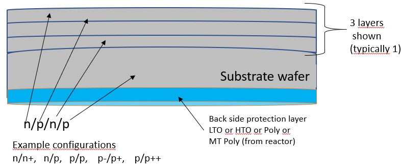
| Back side protection | Reactor types | Silicon sources |
|---|---|---|
| Epitaxial Si layer, during the growth, is doped in a controled way, from gas present in ambient atmosphere. The most common are phosphin (PH3) or diboran (B2H4). However, the dopant atoms also migrate from the substrate to the layer, additionally doping the layer, in unwonted way. To prevent this "auto-doping" phenomaena the wafers shall be protected on the backsides. The protection is made by adding additional layer on the wafer's backside. It can be sealing oxide layer or polysilicon layer or sometimes super sealing oxide and poly together. | In common use there are 3 types of silicon on silicon epi reactors: batch reactors: barrel (where wafers are standing vertically) or pan-cake (wafers are in a horisontal) single wafer reactors (pan-cake type but for one wafer only). |
The sources of silicon for epi are ususally: Trichlorosilan: SiHCl3+H2→↓Si+3HCl Tetrachloride: SiCl4+2H2→↓Si+4HCl The advantage of using SiHCl3 to SiCl4 is lower process temperature about 1090 °C to about 1115 °C adequately. |
Silicon properties
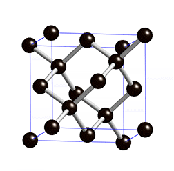
Silicon, Si - the most common semiconductor, single crystal Si can be processed into wafers up to 450 mm in diameter. Wafers are thin (thickness depends on wafer diameter, but is typically less than 1 mm), circular slice of single-crystal semiconductor material cut from the ingot of single crystal semiconductor. All lattice planes and lattice directions are described by a mathematical description known as a Miller Index. In the cubic lattice system, the direction [hkl] defines a vector direction normal to surface of a particular plane or facet. A crystal can always be divided into a fundamental shape with a characteristic shape, volume, and contents.
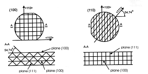
As a crystal is periodic, there exist families of equivalent directions and planes. Notation allows for distinction between a specific direction or plane and families of such. Miller convention:
- Use the [ ] notation to identify a specific direction,
- Use the < > notation to identify a family of equivalent directions,
- Use the ( ) notation to identify a specific plane,
- Use the { } notation to identify a family of equivalent planes.
Crystal Properties
| Property | Value | Units |
|---|---|---|
| Structure | Cubic | |
| Space Group | Fd3m | |
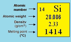
| Atomic weight | 28.0855 | |
| Lattice spacing (a0) at 300K | 0.54311 | nm |
| Density at 300K | 2.3290 | g/cm3 |
| Nearest Neighbour Distance at 300K | 0.235 | nm |
| Number of atoms in 1 cm3 | 4.995×10²² | |
| Isotopes |
28 (92.23%) 29 (4.67%) 30 (3.10%) |
|
| Electron Shells | 1s22s22p63s23p2 | |
| Common Ions | Si 4 +, Si 4 - | |
| Critical Pressure | 1450 | atm |
| Critical Temperature | 4920 | °C |
Band Structure Properties
| Property | Value | Units |
|---|---|---|
| Dielectric Constant at 300 K (Relative Permittivity (εr)) | 11.7 | |
| Dielectric Strength | 100 - 700 | (V/mil) |
| Loss Tangent | 0.005 (at 1 GHz) 0.015 (at 10 GHz) |
|
| Effective density of states (conduction, Nc T=300 K ) | 2.8×10¹⁹ | cm-3 |
| Effective density of states (valence, Nv T=300 K ) | 1.04×10¹⁹ | cm-3 |
| Electron affinity | 133.6 | kJ / mol |
| Energy Gap Eg at 300 K (Minimum Indirect Energy Gap at 300 K) | 1.12 | eV |
| Energy Gap Eg at ca. 0 K (Minimum Indirect Energy Gap at 0K) | 1.17 (at 0 K) | eV |
| Minimum Direct Energy Gap at 300 K | 3.4 | eV |
| Energy separation (EΓL) | 4.2 | eV |
| Intrinsic Debye length | 24 | µm |
| Intrinsic carrier concentration at 300K | 1×10¹⁰ | cm-3 |
| Intrinsic carrier concentration at 25°C | 8.6×10⁹ | cm-3 |
| Intrinsic resistivity | 3.2×10⁵ | Ω×cm |
| Auger recombination coefficient Cn | 1.1×10⁻³⁰ | cm6 / s |
| Auger recombination coefficient Cp | 3×10-31 | cm6 / s |
Temperature dependence of the energy gap:
Eg = 1.17 - 4.73×10⁻⁴×T2/(T+636) (eV)
where: T is temperature in degrees K.
Thermal Properties
| Property | Value | Units |
|---|---|---|
| Melting point |
1414 1687 |
°C K |
| Boiling point | 3538 | K |
| Specific heat | 0.7 | J / (g × °C) |
| Thermal conductivity [300K] | 148 | W / (m × K) |
| Thermal diffusivity | 0.8 | cm2/s |
| Thermal expansion, linear | 2.6×10⁻⁶ | °C -1 |
| Debye temperature | 640 | K |
| Temperature dependence of band gap | -2.3e-4 | eV/K |
| Heat of: fusion / vaporization / atomization | 39.6 / 383.3 / 452 | kJ / mol |
Electrical Properties
| Property | Value | Units |
|---|---|---|
| Breakdown field | ≈ 3×10⁵ | V/cm |
| Index of refraction | 3.42 | |
| Mobility electrons | ≈ 1400 | cm2 / (V × s) |
| Mobility holes | ≈ 450 | cm2 / (V × s) |
| Diffusion coefficient electrons | ≈ 36 | cm2/s |
| Diffusion coefficient holes | ≈ 12 | cm2/s |
| Electron thermal velocity | 2.3×10⁵ | m/s |
| Electronegativity | 1.8 | Pauling`s |
| Hole thermal velocity | 1.65×10⁵ | m/s |
| Optical phonon energy | 0.063 | eV |
| Density of surface atoms |
(100) 6.78 (110) 9.59 (111) 7.83 |
1014/cm2 1014/cm2 1014/cm2 |
| Work function (intrinsic) | 4.15 | eV |
| Ionization Energies for Various Dopants |
Donors: Sb 0.039P 0.045 As 0.054 Acceptors: B 0.045Al 0.067 Ga 0.072 In 0.16 |
eV eV eV eV eV |
Mechanical Properties
| Property | Value | Units | |
|---|---|---|---|
| Bulk modulus of elasticity | 9.8×10¹¹ | dyn/cm2 | |
| Density | 2.329 | g/cm3 | |
| Hardness | 7 | on the Mohs scale | |
| Surface microhardness (using Knoop's pyramid test) | 1150 | kg/mm2 | |
| Elastic constants |
C11 = 16.60×10¹¹ C12 = 6.40×10¹¹ C44 = 7.96×10¹¹ |
dyn/cm2 dyn/cm2 dyn/cm2 |
|
| Young's Modulus (E) |
[100] [110] [111] |
129.5 168.0 186.5 |
GPa GPa GPa |
| Shear Modulus | 64.1 | GPa | |
| Poisson's Ratio | 0.22 to 0.28 | - | |
Resistivity & Mobility Calculator for Semiconductor Silicon
Please note:
- To calculate Resistivity, choose Dopant and enter/modify Dopant Density in the Dopant Density field; the Calculator will compute Type, Resistivity and Mobility in corresponding columns.
- To calculate Dopant Density, choose Dopant and enter/modify Resistivity.
- Concentration and Mobility are always computed; they cannot be entered/modified. Likewise type is a consequence of the Dopant chosen.
Plane Intersection Angle Calculator
References
- Danilo Crippa, Daniel L. Rode, Maurizion Masi [Silicon Epitaxy], Academic Press 2001
- Robert Hull [Properties of Crystalline Silicon], INSPEC 1999
- A. Kelly, G.W. Groves [Crystallography and crystal defects], PWN 1980
- П.С. Кириеев [Физика полупроводников], Высшая школа 1969
- Arjan Ciftja, Thorvald Abel Engh, Merete Tangstad [Refining and Recycling of Silicon: A Review], Norwegian University of Science and Technology 2008
- Tadeusz Penkala [Zarys krystalografii], PWN 1977
- On-line materials from: Bernreuter Research, Green Rhino Energy
-
Semiconductor Nanotechnology: Advances in Information and Energy
Processing and Storage - Nanostructure Science and Technology
Stephen M. Goodnick (editor), Anatoli Korkin (editor), Robert Nemanich (editor), Springer Nature Switzerland AG 2018 - Dunster, David Francis, "Semiconductors for engineers", London, Business Books, 1969
